Samsung Foundry

As part of Samsung's Q1 earnings announcement, the company has outlined some of its foundry unit's key plans for the rest of the year. The company has confirmed that it remains on track to meeting its goal of starting mass production of chips on its SF3 (3 nm-class, 2nd Generation) technology in the second half of the year. Meanwhile in June, Samsung Foundry will formally unveil its SF2 (2 nm-class) process technology, which will offer a mix of performance and efficiency enhancements. Finally, the company the company is preparing a variation of its 4 nm-class technology for integration into stacked 3D designs. SF2 To Be Unveiled In June Samsung plans to disclose key details about its SF2 fabrication technology at the VLSI Symposium 2024 on June...
Samsung Foundry: 2nm Silicon in 2025
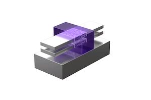
One of the key semiconductor technologies beyond 3D FinFET transistors are Gate-All-Around transistors, which show promise to help extend the ability to drive processors and components to higher performance...
29 by Dr. Ian Cutress on 10/6/2021
Samsung Foundry’s New 17nm Node: 17LPV brings FinFET to 28nm
Despite most discussion about chip manufacturing focusing on the leading edge and blazingly fast and complex side of the industry, the demand for the ‘legacy’ process technologies is also...
11 by Dr. Ian Cutress on 10/6/2021
Samsung Foundry to Almost Double Output by 2026
It’s hard not to notice that we’re in the middle of a semiconductor crunch right now. Factories are running at full steam, but pinch points in the supply chain...
6 by Dr. Ian Cutress on 10/6/2021
Samsung: Deployment of 3nm GAE Node on Track for 2022
Samsung Foundry has made some changes to its plans concerning its 3 nm-class process technologies that use gate-all-around (GAA) transistors, or what Samsung calls its multi-bridge channel field-effect transistors...
32 by Anton Shilov on 7/9/2021
Sales of Fab Tools Surge to Over $71 Billion in 2020
SEMI, an organization representing chipmakers and producers of semiconductor production tools, published this week that sales of wafer processing equipment has surged to an all-time record of $71.19 billion...
18 by Anton Shilov on 4/15/2021
EUV Pellicles Ready For Fabs, Expected to Boost Chip Yields and Sizes
Foundries started limited usage of extreme ultraviolet (EUV) lithography for high-volume manufacturing (HVM) of chips in 2019. At the time, ASML's Twinscan NXE scanners were good enough for production...
35 by Anton Shilov on 3/31/2021
Report: Semi Demand 30% Above Supply, 20% Year-on-Year Growth
Semiconductor foundry offerings are thriving due to unprecedented demand for semiconductors and processors in recent quarters. Analysts from TrendForce believe that in Q1 2021 foundries will increase their revenue...
31 by Anton Shilov on 2/25/2021
Samsung Foundry: New $17 Billion Fab in the USA by Late 2023
Samsung Foundry has filed documents with authorities in Arizona, New York, and Texas seeking to build a leading-edge semiconductor manufacturing facility in the USA. The potential fab near Austin...
36 by Anton Shilov on 2/10/2021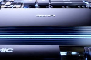
Samsung Announces "X-Cube" 3D TSV SRAM-Logic Die Stacking Technology
Yesterday, Samsung Electronics had announced a new 3D IC packaging technology called eXtended-Cube, or “X-Cube”, allowing chip-stacking of SRAM dies on top of a base logic die through TSVs. Current...
21 by Andrei Frumusanu on 8/14/2020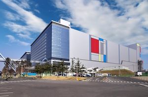
Samsung Starts Mass Production at V1: A Dedicated EUV Fab for 7nm, 6nm, 5nm, 4nm, 3nm Nodes
Samsung Foundry has started mass production of chips using its 6LPP and 7LPP manufacturing processes at its new V1 fab. The new facility employs one of the industry’s first...
30 by Anton Shilov on 2/20/2020
Samsung Kicks Off Mass Production of AI Chip for Baidu: 260 TOPS at 150 W
Samsung Foundry and Baidu this week said that the companies were about to start mass production of an AI accelerator chip early in 2020. Baidu’s Kunlun chip is to...
9 by Anton Shilov on 12/18/2019
New Tools Simplify Development of 2.5D Multi-Die 7nm Designs at Samsung Foundry
Advanced packaging technologies simplify production and increase performance of highly-complex multi-die SoCs as the semiconductor industry is looking at chiplet approach as an alternative to large dies that take...
5 by Anton Shilov on 10/22/2019
Samsung & TSMC Develop 8nm & 7nm Automotive-Grade Nodes
As vehicles are getting ‘smarter’ and gaining autopilot capabilities, it is easy to predict that the demand for higher-performing and more complex automotive SoCs will be growing rapidly in...
29 by Anton Shilov on 10/14/2019
New Tools & IP Accelerate Development of 5nm Arm ‘Hercules’ SoCs
Arm, Synopsys, and Samsung Foundry have developed a set of optimized tools and IP that will enable chip designers to build next-generation SoCs based on Arm’s Hercules processor cores...
9 by Anton Shilov on 10/10/2019
Samsung’s Aggressive EUV Plans: 6nm Production in H2, 5nm & 4nm On Track
Samsung Foundry formally started to produce chips using its 7LPP (7 nm low power plus) fabrication process last October and has not slowdown development of its manufacturing technologies since...
42 by Anton Shilov on 7/31/2019
Samsung’s 5nm EUV Technology Gets Closer: Tools by Cadence & Synopsys Certified
Samsung Foundry has certified full flow tools from Cadence and Synopsys for its 5LPE (5 nm low-power early) process technology that uses extreme ultraviolet lithography (EUV). Full flow design...
13 by Anton Shilov on 7/8/2019
Synopsys to Accelerate Samsung’s 7nm Ramp with Yield Explorer Platform
Synopsys has announced an acceleration of development on its yield learning platform designed to speed up ramp up of chips made using Samsung Foundry’s 7LPP (7 nm low power...
16 by Anton Shilov on 7/4/2019
Samsung to Invest $115 Billion in Foundry & Chip Businesses by 2030
Being among the largest contract makers of semiconductors and among leading developers of chips for various applications, Samsung Electronics wants to become the world’s leader in these industries. To...
27 by Anton Shilov on 4/24/2019
Samsung Completes Development of 5nm EUV Process Technology
Samsung Foundry this week announced that it has completed development of its first-generation 5 nm fabrication process (previously dubbed 5LPE). The manufacturing technology uses extreme ultraviolet lithography (EUVL) and...
21 by Anton Shilov on 4/17/2019
ASML to Ship 30 EUV Scanners in 2019: Faster EUV Tools Coming
ASML said last week that it planned to ship 30 extreme ultraviolet scanners in 2019, up significantly from 2018. The plan is not surprising, as demand for EUV lithography...
17 by Anton Shilov on 1/28/2019


